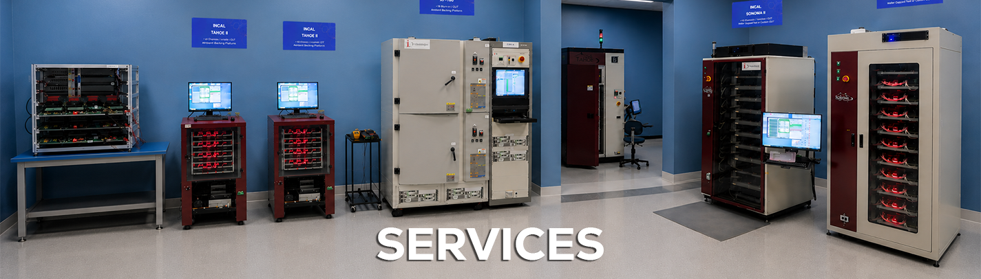
Semiconductor Test & Characterization
Full electrical characterization and functional testing of advanced semiconductor devices across temperature, voltage, and frequency conditions required for aerospace and defense qualification.
- DC parametric and functional test coverage
- Temperature characterization from cryogenic to high-temp
- Custom test program development for complex ASICs
High-Power Device Testing
Specialized test infrastructure for high-power semiconductor devices including GaN, SiC, and high-voltage transistors used in power conversion and RF amplification applications.
- High-current and high-voltage device characterization
- Thermal resistance and power dissipation analysis
- Safe operating area (SOA) evaluation
RF and Millimeter-Wave Validation
Comprehensive RF characterization and millimeter-wave device validation supporting radar, electronic warfare, and satellite communications semiconductor technologies.
- S-parameter and noise figure characterization
- mmWave testing up to 110 GHz
- Load-pull power and linearity measurement
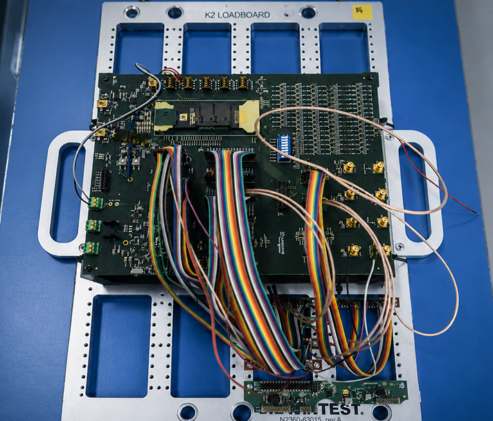
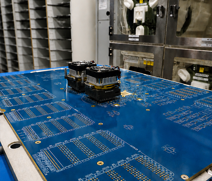
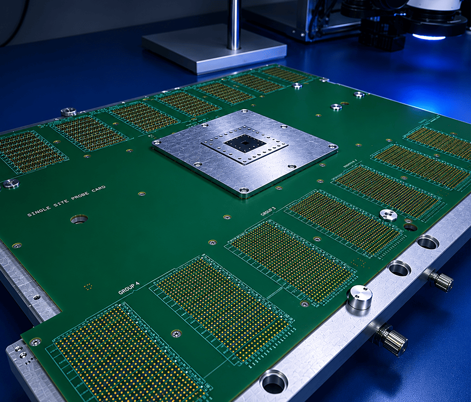
Load Board & Test Hardware Development
Custom load board design and test hardware development enabling precise electrical access to complex semiconductor packages used in aerospace and defense applications.
- Custom PCB design for ATE platforms
- High-frequency signal integrity optimization
- Thermal and mechanical interface engineering
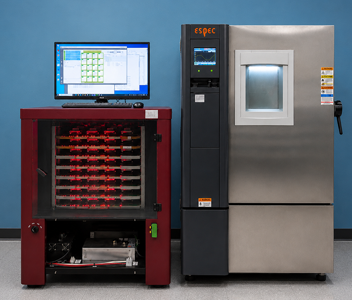
Reliability Screening & Burn-In
Structured reliability screening and burn-in programs designed to identify infant mortality failures and validate long-term device performance in mission environments.
- HTOL, HTSL, and temperature cycling programs
- Pre and post stress electrical testing
- Failure analysis and data reporting
Radiation Validation
Radiation effects evaluation including total ionizing dose (TID) and single event effects (SEE) testing to qualify semiconductor devices for space and high-radiation environments.
- Total Ionizing Dose (TID) evaluation
- Single Event Effects (SEE) characterization
- Radiation hardness assurance (RHA) support
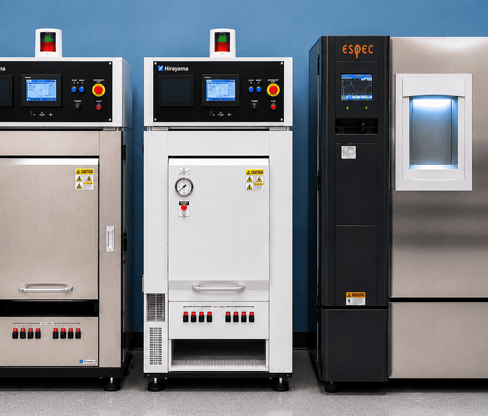
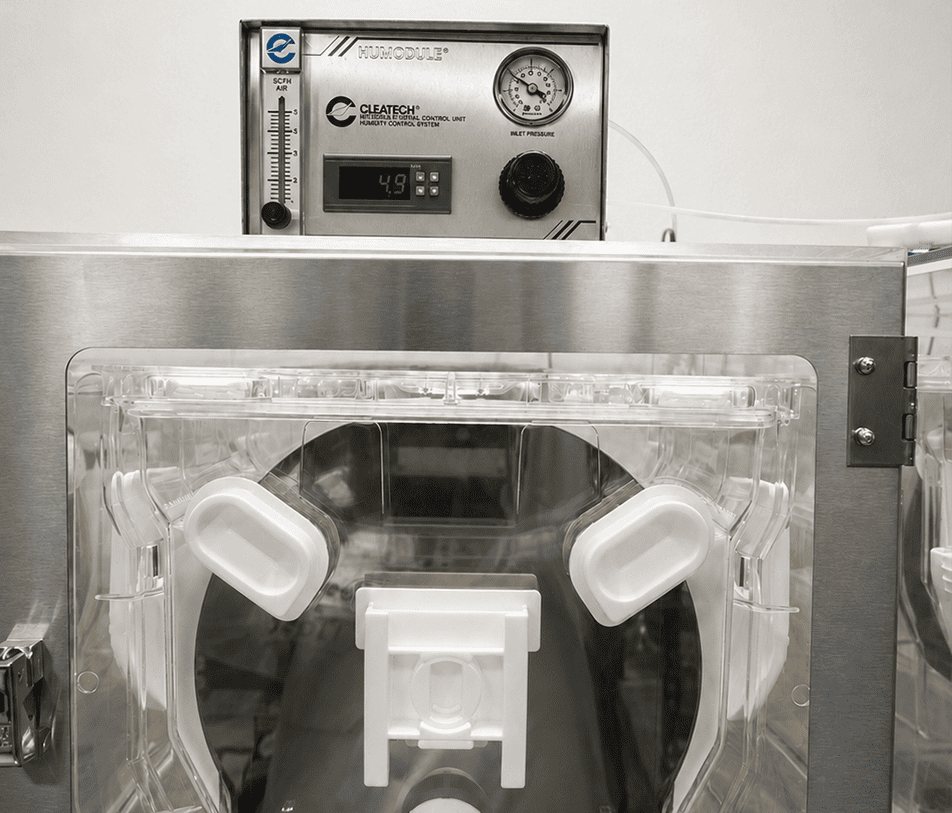
Environmental Testing
Environmental stress testing to validate semiconductor device performance under the thermal, mechanical, and atmospheric conditions encountered in aerospace and defense deployment.
- Thermal shock and temperature cycling
- Vibration, shock, and mechanical stress testing
- Humidity and altitude exposure programs
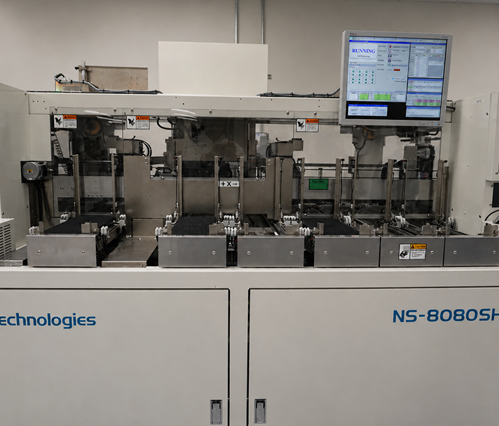
Logistics & Program Lifecycle Support
End-to-end program logistics and lifecycle management supporting semiconductor qualification from initial engineering evaluation through production and sustained program support.
- Program planning and qualification roadmap development
- Inventory management and device traceability
- Long-term program documentation and reporting
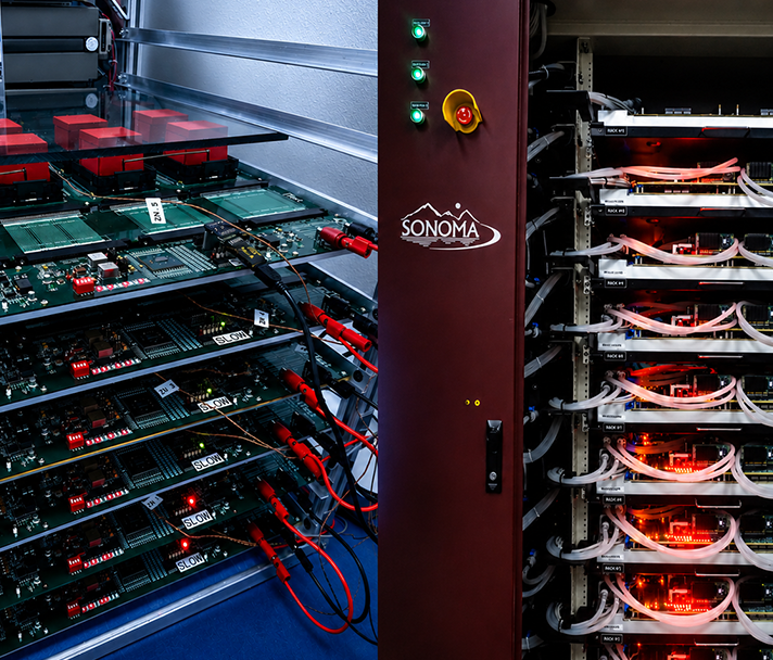
Electrical Test & Characterization
Advanced semiconductor characterization for high-performance devices—from ultra-high pin count and high-speed interfaces through RF and millimeter-wave coverage, high-power evaluation, and wafer sort / probe.
- Ultra-high pin count testing and exascale-class throughput
- High-speed digital interfaces and leading-edge instrumentation
- RF and millimeter-wave characterization; high-power device testing
- Wafer sort and probe; three-temperature wafer sort
- Automation, high throughput, and clean hardware environments
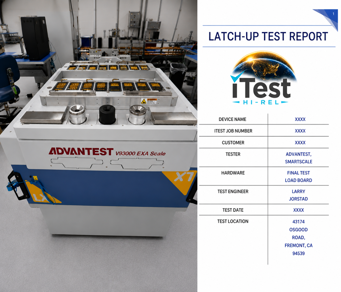
Revolutionizing Latch-Up on ATE
Traditional latch-up methodologies were not designed for today's high-pin-count, multi-domain semiconductor devices. iTest utilizes production-class ATE platforms to perform mission-mode latch-up characterization, automated parametric analysis, and high-current stress testing under realistic operating conditions, providing greater accuracy, observability, and confidence for qualification of advanced semiconductor technologies.
- Production-class ATE platforms for enhanced accuracy and repeatability
- Multi-domain power rail control, monitoring, and synchronized stress application
- Automated pre- and post-stress electrical characterization
- Integrated curve tracing and parametric analysis
- High-current testing for advanced ASICs, FPGAs, and AI devices
- Accelerated qualification cycles with increased confidence in deployment readiness
Hardware & Interface Engineering
Dedicated hardware design and signal integrity engineering for complex ATE and mission interfaces—RF and high-speed connectivity, power and thermal engineering, and intelligent hardware systems.
- Dedicated hardware design and stack-up development
- Signal integrity engineering and RF & interface capability
- Power and thermal engineering for demanding test conditions
- Advanced stack-up design and intelligent hardware systems
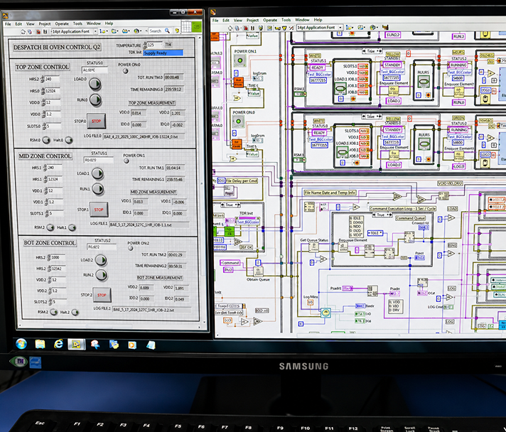
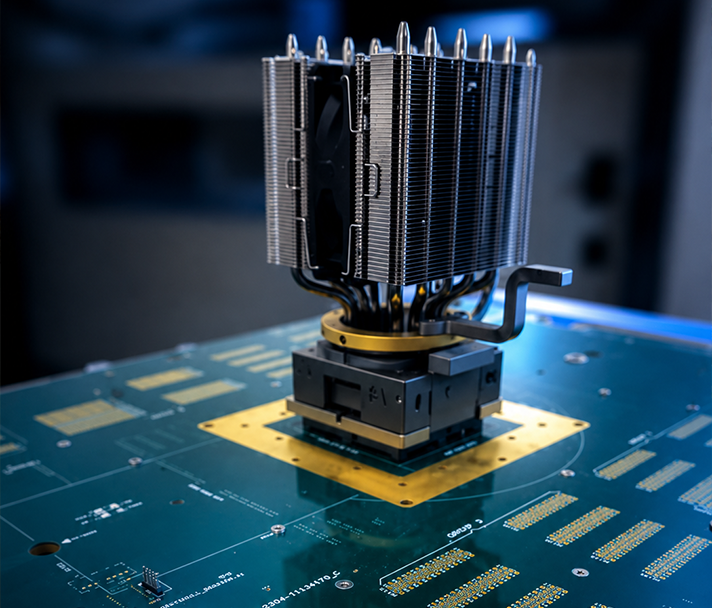
HTOL & Advanced Burn-In
Burn-in treated as a reliability intelligence process—combining high-speed and high-power stress with thermal control, real-time monitoring, and diagnostics to surface early failures before deployment.
- High-speed and high-power burn-in with thermal control
- Real-time monitoring and early failure detection
- Thermal mapping and device-level diagnostics